Microsoft Details Azure Maia 300 Chip for Multi-Gigawatt Rollouts
Built on TSMC's N2P node with 288GB of HBM4, the third-generation inference accelerator is designed to become Microsoft's primary inference engine.
In short
- Microsoft announced Azure Maia 300 on October 12, 2026, targeting multi-gigawatt data center deployments starting in 2027.
- The chip features a multi-chiplet design with a TSMC N2P compute die, eight HBM4 stacks, 288GB memory capacity, and 18 TB/s bandwidth.
- Microsoft claims Maia 300 achieves 40% more tokens per megawatt than leading GPU systems and up to 7x the rack-scale token throughput of Maia 200.
- Maia hardware is reserved exclusively for Microsoft internal services, including Copilot and proprietary MAI models, rather than external Azure rentals.
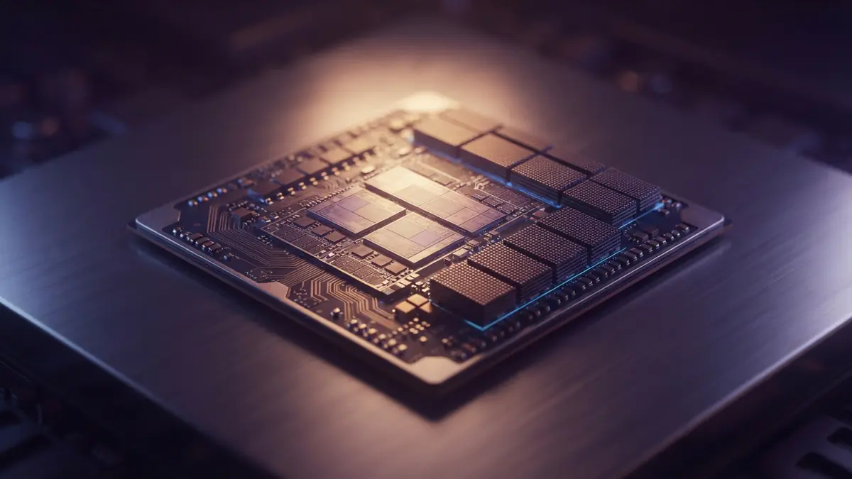
On October 12, 2026, Microsoft introduced the Azure Maia 300, its third-generation custom artificial intelligence accelerator engineered to power cloud-scale inference workloads. Unveiled at the OCP Global Summit, the accelerator pairs an advanced semiconductor manufacturing node with high-bandwidth memory to serve large-scale reasoning and multi-step agentic systems. According to The Official Microsoft Blog, Microsoft plans to expand the Azure Maia family into multi-gigawatt deployments starting in 2027, positioning Maia as the primary AI inference infrastructure across its enterprise and consumer products.
The announcement reflects Microsoft's broader strategy to expand internal silicon production and reduce dependency on external hardware suppliers. Satya Nadella, Microsoft's chief executive officer, described the development as the company's "biggest bet yet on our own silicon," as reported by GeekWire. By designing accelerators tailored specifically to its proprietary software stack, Microsoft aims to navigate power grid constraints that dictate the pace of AI infrastructure expansion.
Multi-Chiplet Architecture in Azure Maia 300 Built on TSMC N2P
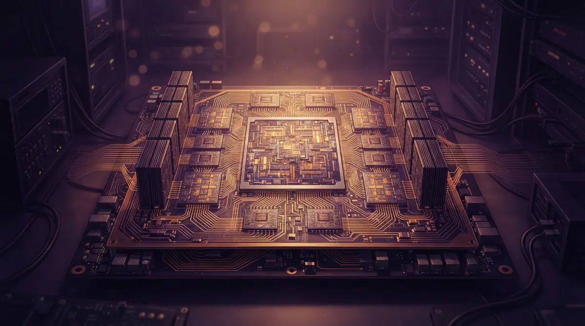
Unlike its predecessor, the Maia 200, which relied on a monolithic N3P die, the Azure Maia 300 shifts to a disaggregated multi-chiplet design. As detailed in the Microsoft Azure Blog, the accelerator isolates compute tasks onto a die fabricated on Taiwan Semiconductor Manufacturing Co.'s (TSMC) N2P node. Memory controllers and input/output functions are moved to separate dies optimized for connectivity, bandwidth, and manufacturing cost. This modular arrangement increases the silicon area allocated strictly to compute calculations, boosting compute floating-point operations by 36%.
Memory specifications show significant gains aimed at addressing decode-heavy model architectures. According to technical documentation analyzed by StorageReview, each Maia 300 accelerator incorporates eight HBM4 stacks providing 288GB of capacity and 18 TB/s of peak memory bandwidth, running within a 950-watt thermal design power (TDP) envelope. Compared to the Maia 200's 216GB of HBM3E and 7.1 TB/s bandwidth, the new design delivers 2.5 times the memory bandwidth, a 33% increase in memory capacity, and approximately double the HBM bandwidth per watt.
To manage data movement inside the package, Microsoft transitioned from uniform memory access to a locality-aware non-uniform memory access (NUMA) architecture across the chiplets. Built around an evolution of Microsoft's Software Defined Locally Accessed Dataflow Architecture (SDLA), the system allows software to coordinate data placement across on-die SRAM scratchpads, DMA engines, and high-bandwidth memory. Narrower numerical formats, including enhanced MXFP4 and sub-3-bit storage formats, further minimize memory footprint and data traffic during inference execution.
Scaling Density: 96 Accelerators in a 167-Kilowatt Rack
At the data center level, Microsoft redesigned its physical server topology to maximize density within strict thermal and electrical parameters. As outlined in the Microsoft Azure Blog, the Maia 300 system integrates 96 accelerators across 24 four-accelerator trays into a single 167-kilowatt rack. This doubles the accelerator density of the 48-chip Maia 200 rack while providing 27.6TB of HBM capacity and 1.7 PB/s of aggregate memory bandwidth per rack.
The system utilizes a hybrid cooling approach, where custom liquid cooling loops capture more than 80% of the thermal load generated by the accelerators, voltage regulator modules, and switch application-specific integrated circuits (ASICs). The remaining heat from memory, storage, and auxiliary server components is dissipated using air cooling. Power distribution relies on dual power feeds and a 50-volt busbar infrastructure with integrated transfer switches to maintain system uptime during maintenance operations.
Scale-up networking extends beyond single rack enclosures through a two-tier Ethernet fabric, as documented by StorageReview. Each accelerator incorporates an integrated AI network controller with 32 ports of 400 Gb/s Ethernet running a proprietary AI transport protocol. Within a rack tray, direct electrical links connect paired accelerators, while six high-radix switch ASICs connect all 96 units in the rack pod. Optical connections then link up to 128 racks together, forming a scale-up superpod spanning up to 12,288 accelerators under a unified communication model.

Production Workloads and Internal Deployment Timeline
Microsoft intends to deploy the Azure Maia 300 in production facilities beginning in 2027. According to reporting by The Verge, executive vice president Scott Guthrie noted that Microsoft expects Maia 300 to achieve 40% more tokens per megawatt compared to leading GPU-based systems, while yielding up to seven times the rack-scale token throughput of Maia 200.
The Maia architecture is specifically aligned with Microsoft's internal product roadmap rather than external commercial cloud rentals. While The Verge reported that Maia 300 could help Microsoft catch competitors in frontier AI, Microsoft AI chief executive officer Mustafa Suleyman emphasized the need for a platform the company owns and co-designs with Microsoft AI models. While second-generation Maia 200 accelerators currently serve production workloads across the United States, Europe, and Australia for Microsoft Copilot, GitHub Copilot and Microsoft Foundry deployments will expand before the close of 2026, laying the software foundation for the Maia 300 transition.
Despite heavy capital allocation toward proprietary silicon, Microsoft maintains established supply agreements with external semiconductor vendors. Nadella confirmed that the company will deploy next-generation systems utilizing Nvidia's Vera Rubin and AMD's Helios architectures. Analysis by Evercore ISI reported by GeekWire estimates that custom Maia silicon will represent roughly 10% of Microsoft's total AI chip spending by early 2027. Further technical demonstrations and deployment roadmaps will be presented at Microsoft Ignite in November 2026.
Questions people ask
When will Microsoft deploy Azure Maia 300?
Microsoft plans to begin production deployments of Azure Maia 300 in 2027 across multi-gigawatt data center installations.
Can external developers rent Azure Maia 300 instances?
No. Microsoft reserves Maia silicon exclusively for its own internal workloads, including Microsoft Copilot, GitHub Copilot, and internal model development, rather than offering it for cloud rental.
How does Maia 300 compare to Maia 200 in hardware specifications?
Maia 300 provides 288GB of HBM4 memory (up from 216GB HBM3E), 18 TB/s bandwidth (up from 7.1 TB/s), and doubles rack density to 96 accelerators per 167 kW rack, compared to 48 accelerators in Maia 200.
Sources
- Before - Microsoft's latest custom chip: Maia 300Microsoft's latest custom chip: Maia 300, Oct 12, 2026, official source
- Deep dive into Azure Maia 300 architectureMicrosoft Azure Blog, Oct 12, 2026, official source
- Microsoft to expand Azure Maia system to multi-gigawatt deploymentsThe Official Microsoft Blog, Oct 12, 2026, official source
- Microsoft’s new AI chip makes it less reliant on Nvidia’s GPUsThe Verge, Oct 12, 2026
- Microsoft plans to scale its own Maia AI chips to gigawatt levels by 2027The Decoder, Oct 12, 2026
- Microsoft makes 'biggest bet yet' on its own silicon, unveils new AI chip to reduce reliance on Nvidiageekwire.com, Oct 12, 2026
- Microsoft Maia 300 Puts 288GB of HBM4 at 18TB/s on an N2P Chiplet and 96 Accelerators in a 167kW RackStorageReview.com, Oct 12, 2026
How this story was made: the newsroom picked it up from news.microsoft.com, Google News and Google Search, gathered the full text of the sources above, and drafted it with AI assistance. Every factual claim was then checked against those sources before publishing (40 claims checked). Illustrations marked as AI-generated are not photographs. Spotted an error? Tell us.
Published October 13, 2026 at 00:23 UTC